COMPUTER SIMULATION OF P-N JUNCTION DEVICES
N.Sanjay Rebello, Chandramouli Ravipati, Dean A. Zollman, and Lawrence T. Escalada
Kansas State University, Physics Department, 116 Cardwell Hall, Manhattan, KS 66506-2601
ABSTRACT
We present here a computer program – the Semiconductor Device Simulator which simulates the working of three p-n junction devices - the LED, the solar cell, and the tunnel diode. This program enables students to create the device starting with two pieces of intrinsic semiconductor material, and doping them appropriately to create a p-n junction device of their choice. While creating the device, students can observe the changes in the energy bands and Fermi level as a response to doping. The device once created, can then be incorporated into a circuit where the students can observe the energy bands, the I-V graph, as well as the intensity spectrum of the device in response to the changes in applied voltage and/or incident light. No prior knowledge of higher level mathematics is required to use the program. The program is available for WindowsÔ and MacintoshÔ platforms. The flexibility of the program allows it to be used by students over a range of academic levels. We have field tested the program along with associated materials in both high school and university environments. The current version of the program contains modifications based on these field tests.
I. INTRODUCTION
The Visual Quantum Mechanics1,2 project is developing materials to help students learn quantum physics. The primary audience for these materials is high school or introductory undergraduate students who do not have a background in higher level mathematics or quantum physics. To reach these students we are concentrating on the development of activities which integrate hands-on experiments, computer visualizations, and multimedia materials in addition to the more traditional written materials.
During the first eight months of this project we have concentrated on developing activities with a device that requires knowledge of quantum physics to understand how it works. The ubiquitous light emitting diode (LED) is recognized by almost every student as a small red or green light that indicates that some electronic gadget such as a CD player or computer disk drive is operating. To capitalize on this recognition, we are have designed and tested a series of activities that will enable the students to qualitatively explain how an LED is able to emit light. Since the primary goal of the activities is to enable students to understand the quantum effects in an LED, the students must be able to understand the relationship between the energy bands of the material of an LED and its electrical and spectral characteristics. To understand this relationship the students must learn how the energy bands respond to changes in applied voltage or incident light. Most standard introductory texts do not mention the quantum properties of LEDs or any similar devices. More advanced texts discuss these devices quantitatively, and use relatively few visualization tools. Hence these books and other instructional materials are unsuitable for our intended audiences.
This lacuna in the available instructional materials motivated us to develop a computer program that would enable a user who has no knowledge of higher level mathematics or physics to understand how the electrical and spectral properties of a p-n junction device can be explained using energy bands. Although the original purpose of the program was to explain how an LED worked, we decided that it could be designed to address the operation of any p-n junction device. Also while the program was originally meant for users who do not have a knowledge of semiconductor physics, the program in its current version can be used by students studying solid state physics, semiconductors or electronics at a higher level.
II. PROGRAM DESCRIPTION
The program begins by displaying two cubes on either side of the screen. These cubes represent two pieces of intrinsic semiconductor material, as shown in Figure 1. Although the default semiconductor is silicon, the user can choose from a range of commonly used semiconductors. Advanced users can also "create" their own hypothetical semiconductor with any desired energy gap, electron and hole mobilities, effective masses and some other parameters. The energy band diagram showing the conduction band edge (Ec), the valence band edge (Ev), and the Fermi energy (Ef) for the intrinsic semiconductor is displayed directly below each corresponding cube. The user can also change the temperature to observe the changes in Fermi energy.
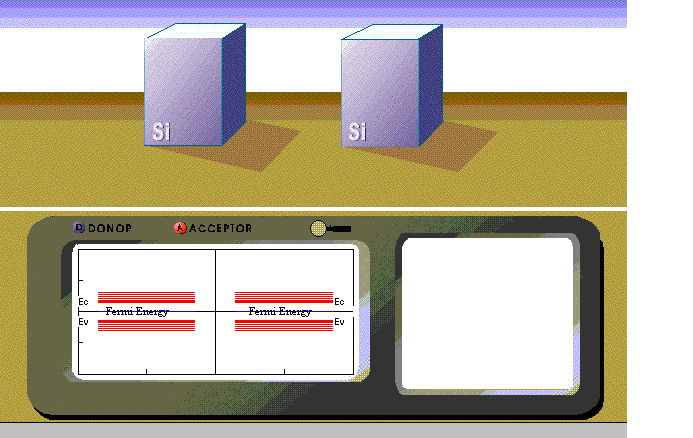
Figure 1: The opening screen of the Semiconductor Device Simulator program showing the two semiconductor (silicon) blocks and the energy bands below each. Silicon is the default semiconductor although others can be chosen using the "Device" menu.
Next, the user adds dopant atoms to each of the semiconductor blocks. A p-type material is represented by addition of acceptors and an n-type material is represented by addition of donors (See Figure 2). If acceptors are added to the left cube and donors are added to the right cube, the left cube becomes a p-type semiconductor and the right cube becomes an n-type semiconductor. The user can also see a representation of the internal atomic structure of a p-type or n-type semiconductor that reveals the acceptor or donor atom within the semiconductor lattice structure, as shown in Figure 2. The Fermi energy of the side where acceptors are added decreases and becomes closer to the valence band edge, while those on the side where donors are added increases and becomes closer to the conduction band edge. By adding a single acceptor or donor, the user increments the carrier concentration (p or n respectively) by a fixed amount.
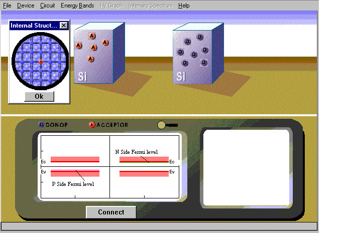
Figure 2: The two semiconductor blocks after the Acceptor (A) and Donor (D) atoms are added to the each. The inset shows the internal atomic structure with acceptor atoms, viewed using the magnifying tool. Addition of each A or D increments the acceptor and donor concentration respectively by 1x10²² m-3.
Having doped the two sides of the blocks of semiconductor material appropriately (i.e. one is p-type and the other n-type), the user can then bring the two blocks in physical contact with one another, and make the Fermi levels coincide. The energy bands on either side would consequently be misaligned. (See Figure 3) The misalignment depends upon the degree of doping on either side, and is responsible for the built-in potential.
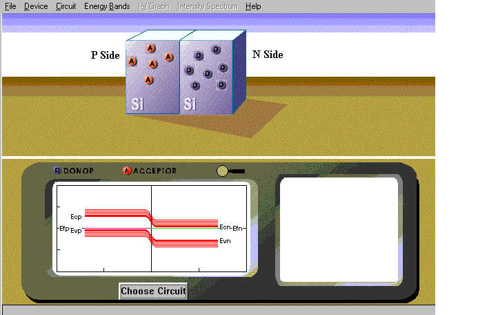
Figure 3: When Fermi levels are aligned, the energy bands are no longer aligned. The acceptor concentration on the left is 4x10²² m-3, while the donor concentration on the right is 7x10²² m-3.
Having created the p-n junction the user can now choose to use it in any of the three devices -- LED, solar cell, or tunnel diode. For the LED and tunnel diode, the users can either place the device in an ideal simple circuit where they control the applied voltage across it with a scroll bar, or they place it in a more realistic circuit with a battery, a resistor, and a potentiometer. The potentiometer appears as a small box with a circular knob (See Figure 5). The users can change the setting of the potentiometer, by clicking and dragging the dot on the knob (i.e. "rotating" the knob). In response to these changes, the voltage across the device, and the current through it will change. In either mode the user can observe changes in the energy bands of the device, which appear directly below the circuit. The user can also observe the current versus voltage graph of the device which appears at the bottom right of the screen. If the device is used in the simple circuit with a scroll bar, the user can observe the complete I-V graph (i.e. both negative and positive), by moving the scroll bar to negative and positive voltages respectively (See Figure 4). In this sense the scroll bar represents an ideal voltage source. It would be similar to connecting the device across a curve tracer or some other more sophisticated equipment. The device used in a circuit with a potentiometer more closely resembles a real situation. Hence, it will not be possible for the viewer to observe both the positive and negative aspects of the I-V graph simultaneously, because in real life one would have to change the polarity of the battery midway to do that.
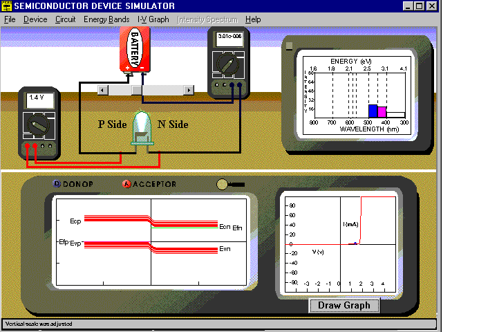
Figure 4: The screen for the Simple Circuit option for the LED. The dopant density on both the n and p sides of this GaP (Gallium Phosphide) LED is 6x10²² m-3. The I-V graph is simulated for a device with a junction area of 5x10⁷ m-2, at a 27°C.
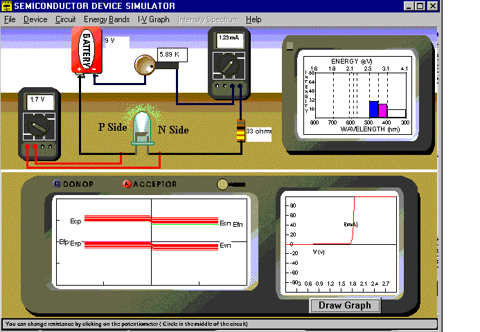
Figure 5: The screen for the LED with Resistance option for the LED. The dopant density on both the n and p sides of this GaP (Gallium Phosphide) LED is 6x10²² m-3. The I-V graph is simulated for a device with a junction area of 5x10⁻⁷ m-2, at a 27°C.
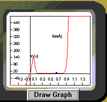
The most significant difference between the I-V graphs for the two situations can be observed for the tunnel diode. When the tunnel diode is placed in a simple circuit with a scroll bar representing an ideal voltage source, the I-V graph is complete with a peak and a valley. When the tunnel diode is in a simple circuit with a scroll bar representing a variable battery, the resulting I-V curve (Figure 6a) resembles one measured by an instrument such as a curve tracer with a very high impedance, so that it is possible to vary the voltage across the device without affecting the current through it. This I-V graph shows the peak and valley voltage of the tunnel diode when it is forward biased.
(a) (b)
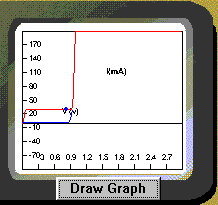
Figure 6: The I-V graphs for the tunnel diode in (a) the Simple Circuit option (b) Tunnel Diode with Resistance option. For both (a) and (b), the dopant density is 5x10²² m-3 on both the n and p sides of this silicon tunnel diode. Both I-V graphs are simulated for devices with a junction area of 5x10⁻⁷ m-2, at 27°C.
When the tunnel diode is in the circuit with a potentiometer, however, the I-V graph (Figure 6b) corresponds to a situation in which the current and not the voltage is being regulated. This situation arises because the potentiometer is a current controller. So at voltages between the peak and valley voltages, the current remains constant at the peak value, unlike the earlier case where the current decreases in going from the peak to the valley. When the potentiometer is being "rotated" in the opposite direction to decrease the current, no increase in current is observed in between the valley and peak voltages. In addition, the current remains at its lower valley value before going to zero at 0V. Hence, in case of the tunnel diode the I-V graphs are not the same for increasing and decreasing current.
In case of the LED the user can also observe the spectrum of the emitted light, which appears at the top right of the screen (See Figure 4). The intensity of the emitted light is proportional to the current through the LED, while the color of the emitted light depends upon the energy gap of the material of the LED. For simplicity, the program assumes an ideal, though unrealistic situation in which no transitions occur to or from intermediate states in the band gap. Hence the lowest energy of the emitted light is the energy of the band gap. Wavelengths corresponding to higher energies are emitted with lower intensities which are proportional to the lower occupancies of the initial and final states corresponding to these energies.
Besides the LED and the tunnel diode, the p-n junction can also be used as solar cell. The solar cell can operate in two modes: the output measurement mode or the circuit mode. In the output measurement mode, the user observes either the open circuit voltage or the short circuit current generated by the solar cell when a user-defined spectrum of light is incident on it. The user can control the intensities of various colors of light that are incident on the solar cell by clicking in the appropriate intensity spectrum that appears at the bottom right of the screen (See Figure 7). A flash light appears with light of the appropriate color, depending upon the color and intensities chosen by the user in the intensity spectrum (See Figure 7). When used in the circuit with a battery and a potentiometer the user can observe the I-V graph of the solar cells for different intensities of light to see the effect of the intensity spectrum (See Figure 8)
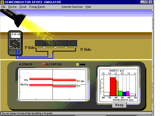
Figure 7: Screen for the Output Measurement option of the solar cell in the short circuit current mode. Both sides of the GaAs solar cell are doped at 6x10²² m-3. The solar cell is primarily irradiated with red light.
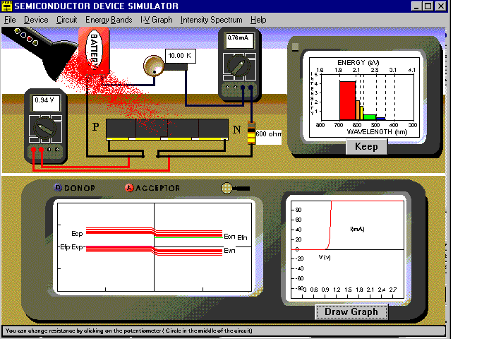
Figure 8: Screen for the Solar Cell in Circuit mode. Both sides of the GaAs solar cell are doped at 6x10²² m-3. The solar cell is primarily irradiated with red light.
The program provides the user with complete flexibility over the parameters. For instance, the user can switch between two devices midway through the simulation, while keeping other parameters the same. Or the user can study how the I-V graph or intensity spectrum would be different if a different semiconductor were used instead or if the doping density or temperature or junction area were different. In case of the LED, if the material chosen is one that is not usually used to make LEDs (e.g. Si due to its relatively small band gap), the program will display a message apprising the user of this difficulty. In case of the tunnel diode, the doping density has to be above a certain threshold value so that the p and n sides are degenerately doped i.e. the Fermi level on the p-side is below the valence band and the Fermi level on the n-side is above the conduction band. The program will prompt the user to ensure that the doping is appropriate for the device p-n junction device to function as a tunnel diode.
III. MODELLING THE SEMICONDUCTOR DEVICES
The equations that describe the physics of a p-n junction device can be found in books on solid state physics3-4 or semiconductor devices5-6. Here we will present a summary of some of the equations used in the simulation.
Calculating the Fermi Energies and Built-in Voltage
The first task is to calculate the Fermi energies of the p and n side, as they change in response to the addition of acceptors and donors respectively. The intrinsic Fermi energies on either side are given by:
 (1)
where:
(1)
where:
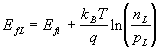
 and
and  (2)
and the symbols have their usual meanings.
The electron and hole effective masses (me and mh), depend upon the semiconductor chosen by the user. The default value of the temperature T, is 300K but can be changed by the user. The values of the Nc and Nv are calculated by the program as per equation (2) and the Fermi energy of the intrinsic material is calculated using equation (1) and displayed in the energy band diagram on the screen.
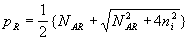
When acceptor and donor atoms are added, the Fermi energies change so that the side which has more acceptors than donors is n-type and the one with more donors than acceptors is p-type. Thus for both the semiconductor blocks, on the left (L) and right (R) we have :
(2)
and the symbols have their usual meanings.
The electron and hole effective masses (me and mh), depend upon the semiconductor chosen by the user. The default value of the temperature T, is 300K but can be changed by the user. The values of the Nc and Nv are calculated by the program as per equation (2) and the Fermi energy of the intrinsic material is calculated using equation (1) and displayed in the energy band diagram on the screen.
When acceptor and donor atoms are added, the Fermi energies change so that the side which has more acceptors than donors is n-type and the one with more donors than acceptors is p-type. Thus for both the semiconductor blocks, on the left (L) and right (R) we have :
 and
and 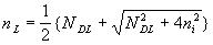 (3)
(3)
 and
and 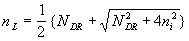 (4)
(4)
where p and n stand for the electron and hole concentrations, and NA and ND are the acceptor and donor concentrations on either side. Equations (3) and (4) are valid only if the n type material is doped only with donors and the p type material is doped only with acceptors. These equations are not valid for partially compensated semiconductors. The values of NA and ND change when the user places donor and acceptor "atoms" in the two cubes representing the two pieces of intrinsic semiconductor on the screen. Each time the user adds a donor or acceptor "atom" the value of NA and ND are incremented by a fixed amount.
The intrinsic carrier concentration, ni is given by:
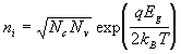 (5)
Then, the Fermi energies on each side are given by:
(5)
Then, the Fermi energies on each side are given by:
 on the left, (6)
and
on the left, (6)
and 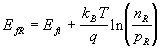 on the right (7)
At room temperature (T=300K) the intrinsic Fermi energy is almost 0eV, so that after doping the side with the positive Fermi energy is the n - side and the one with the negative Fermi energy is the p - side. The program displays the Fermi energies on either side of the energy band diagram (See Figure 2)
When the two blocks of doped semiconductor are brought together the built in voltage across the p-n junction is:
on the right (7)
At room temperature (T=300K) the intrinsic Fermi energy is almost 0eV, so that after doping the side with the positive Fermi energy is the n - side and the one with the negative Fermi energy is the p - side. The program displays the Fermi energies on either side of the energy band diagram (See Figure 2)
When the two blocks of doped semiconductor are brought together the built in voltage across the p-n junction is:
 (8)
If VB is positive then the block on the left is n-doped and the one on the right is p-doped.
If VB is negative then the block on the left is p-doped and the one on the right is n-doped.
The built-in voltage is represented by the fact that when Fermi energies on the p-side and n-side are equilibrated, the energy bands on the two sides are not. This difference in the energy bands on the two sides is visible in the energy band diagram on the screen (See Figure 3)
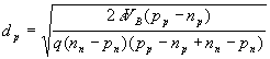
Calculating the depletion widths and band edges within the depletion region
The widths of the depletion region are calculated using the value of the built-in voltage
(8)
If VB is positive then the block on the left is n-doped and the one on the right is p-doped.
If VB is negative then the block on the left is p-doped and the one on the right is n-doped.
The built-in voltage is represented by the fact that when Fermi energies on the p-side and n-side are equilibrated, the energy bands on the two sides are not. This difference in the energy bands on the two sides is visible in the energy band diagram on the screen (See Figure 3)
Calculating the depletion widths and band edges within the depletion region
The widths of the depletion region are calculated using the value of the built-in voltage
 (9)
(9)

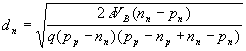 (10)
where the symbols have their usual meanings.
The value of the conduction band edge for the region within the two depletion layers
(10)
where the symbols have their usual meanings.
The value of the conduction band edge for the region within the two depletion layers
 (11)
(11)
 (12)
Equations (11) and (12) assume that the p side is to the left of the junction and the n side is to the right of the junction. The equations for a case where this situation is reversed will be similar to the equations above.
The valence band edges in the depletion layer can then be calculated :
(12)
Equations (11) and (12) assume that the p side is to the left of the junction and the n side is to the right of the junction. The equations for a case where this situation is reversed will be similar to the equations above.
The valence band edges in the depletion layer can then be calculated :
 (13)
The band edges, once calculated from equations (12) and (13) are displayed in the energy band diagram on the screen as shown in Figure 3. The quadratic dependence of the energy band edge on position is indicated in the gradual transition in energy bands in going from the p-side to the n-side.
The I-V characteristics of an LED
When the viewer applies a voltage, VA across the LED, by moving the scroll bar in the "Simple Circuit" option (See Figure 5), the band structure changes and current flows through it depending upon the polarity of the voltage. The change in the energy bands is calculated by simply recalculating the depletion layer widths and band edges with the built-in voltage reduced or increased by the applied voltage so that the new value of the built-in voltage is:
(13)
The band edges, once calculated from equations (12) and (13) are displayed in the energy band diagram on the screen as shown in Figure 3. The quadratic dependence of the energy band edge on position is indicated in the gradual transition in energy bands in going from the p-side to the n-side.
The I-V characteristics of an LED
When the viewer applies a voltage, VA across the LED, by moving the scroll bar in the "Simple Circuit" option (See Figure 5), the band structure changes and current flows through it depending upon the polarity of the voltage. The change in the energy bands is calculated by simply recalculating the depletion layer widths and band edges with the built-in voltage reduced or increased by the applied voltage so that the new value of the built-in voltage is:
 (14)
where VA is the applied voltage, which is positive if the junction is forward biased and negative if the junction is reverse biased. Thus, in case of a forward biased p-n junction the effective built-in voltage barrier is decreased while for the reverse biased case, the built in voltage barrier is increased.
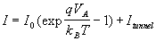
The current across the p-n junction for both the forward and reverse biased cases is given by:
(14)
where VA is the applied voltage, which is positive if the junction is forward biased and negative if the junction is reverse biased. Thus, in case of a forward biased p-n junction the effective built-in voltage barrier is decreased while for the reverse biased case, the built in voltage barrier is increased.
The current across the p-n junction for both the forward and reverse biased cases is given by:
 (15)
where
(15)
where 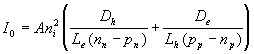 (16)
where:
A= Junction area
Le,h = Effective diffusion length for electrons or holes.
(16)
where:
A= Junction area
Le,h = Effective diffusion length for electrons or holes.
 is the diffusion constant for electrons, where µe is the electron mobility.
 is the diffusion constant for holes, where µh is the hole mobility.
For most widely used semiconductors, the mobility varies as T-4/2
The current calculated in equation (15) is plotted in the I-V graph at the bottom right corner of the screen as shown in Figure 5.
When the LED is in a circuit with a battery, a potentiometer, and another fixed resistance (See Figure 4), the user changes the voltage by "rotating" the knob of the potentiometer. The voltage of the battery is shared by the LED, the potentiometer, and a fixed resistance.
is the diffusion constant for holes, where µh is the hole mobility.
For most widely used semiconductors, the mobility varies as T-4/2
The current calculated in equation (15) is plotted in the I-V graph at the bottom right corner of the screen as shown in Figure 5.
When the LED is in a circuit with a battery, a potentiometer, and another fixed resistance (See Figure 4), the user changes the voltage by "rotating" the knob of the potentiometer. The voltage of the battery is shared by the LED, the potentiometer, and a fixed resistance.
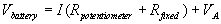 (17)
where ‘I’ is the current through all three elements, however is the same because they are in series, and VA is the voltage that appears across the LED.
Since the current ‘I’ is through the LED, it will depend upon the voltage that appears across the LED, so that
(17)
where ‘I’ is the current through all three elements, however is the same because they are in series, and VA is the voltage that appears across the LED.
Since the current ‘I’ is through the LED, it will depend upon the voltage that appears across the LED, so that
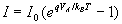 (18)
(18)
The program solves equation (17) and (18) simultaneously in order to determine the current and the voltage appearing across the LED, and display them in the multimeters on the screen. The program uses these quantities to plot the I-V graph for the device which appears at the bottom right of the screen as shown in Figure 5.
The Intensity Spectrum of the LED
The intensity spectrum that is displayed on the screen reflects the relative intensities by dividing the light spectrum (including infrared and ultraviolet) into seven different colors of light. The relative intensity for each of the seven colors is proportional to the product of the electron occupancy of the energy level in the conduction band and the corresponding hole occupancy of an energy level in the valence band at an energy less than the conduction band electron energy by an amount equal to the energy of the emitted light. Thus the relative intensity as a function of energy is given by:
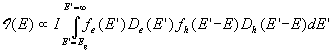 (19)
where :
I is the current flowing through the LED as calculated in equation (15) or (18).
f(E)= Fermi function for electrons or holes.
D(E) = Density of states function for electrons or holes.
The programs determines the intensity value corresponding to each of the seven energy values corresponding to the colors of the visible spectrum, infrared and ultraviolet, and displays the intensity for each in the graph at the top right of the screen (See Figures 4 and 5).
The Illumination Current of the Solar Cell
The current through the solar cell due to the incident light depends upon the energy of the incident light as well as the energy gap of the material of the solar cell:
(19)
where :
I is the current flowing through the LED as calculated in equation (15) or (18).
f(E)= Fermi function for electrons or holes.
D(E) = Density of states function for electrons or holes.
The programs determines the intensity value corresponding to each of the seven energy values corresponding to the colors of the visible spectrum, infrared and ultraviolet, and displays the intensity for each in the graph at the top right of the screen (See Figures 4 and 5).
The Illumination Current of the Solar Cell
The current through the solar cell due to the incident light depends upon the energy of the incident light as well as the energy gap of the material of the solar cell:
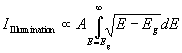 (20)
where A is the area of illumination, and E is the energy of the incident photon.
The user changes the energy of the incident light in the program by clicking in the desired region of the intensity spectrum at the bottom right of the screen (See Figure 7). The vertical position of the click determines the intensity and the horizontal position determines the color and energy of light.
According to equation (20), there is no illumination current when the energy, E of the incident light is less than the energy gap.
The short circuit current, which is the current through a resistance free wire joining the two terminals of the solar cell is:
(20)
where A is the area of illumination, and E is the energy of the incident photon.
The user changes the energy of the incident light in the program by clicking in the desired region of the intensity spectrum at the bottom right of the screen (See Figure 7). The vertical position of the click determines the intensity and the horizontal position determines the color and energy of light.
According to equation (20), there is no illumination current when the energy, E of the incident light is less than the energy gap.
The short circuit current, which is the current through a resistance free wire joining the two terminals of the solar cell is:
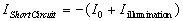 (21)
and the open circuit voltage, which is the voltage across the two terminals of the solar cell when they are disconnected is:
(21)
and the open circuit voltage, which is the voltage across the two terminals of the solar cell when they are disconnected is:
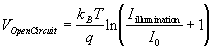 (22)
where I0 is given by equation (16).
The short circuit current or open circuit voltage as computed in equations (21) and (22) respectively, is displayed in the multimeter that is connected across the terminals of the solar cell, as shown in Figure 7. The user can choose whether to display the short circuit current or open circuit voltage.
When the solar cell is in a circuit with a battery, a potentiometer, and another fixed resistance (See Figure 8), the voltage of the battery is shared by the solar cell, the potentiometer, and fixed resistance.
(23)
where I is the current through all three elements, and VA is the voltage that appears across the solar cell.
Since the current I is through the solar cell, it will depend upon the voltage that appears across the solar cell and also the illumination current as determined by equation (20), so that
(22)
where I0 is given by equation (16).
The short circuit current or open circuit voltage as computed in equations (21) and (22) respectively, is displayed in the multimeter that is connected across the terminals of the solar cell, as shown in Figure 7. The user can choose whether to display the short circuit current or open circuit voltage.
When the solar cell is in a circuit with a battery, a potentiometer, and another fixed resistance (See Figure 8), the voltage of the battery is shared by the solar cell, the potentiometer, and fixed resistance.
(23)
where I is the current through all three elements, and VA is the voltage that appears across the solar cell.
Since the current I is through the solar cell, it will depend upon the voltage that appears across the solar cell and also the illumination current as determined by equation (20), so that
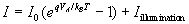 (24)
The current (I) vs. voltage (VA) graph computed using equation (23) the bottom left of the screen (See Figure 8).
The I-V Characteristics of a Tunnel Diode
A p-n junction can function as a tunnel diode, only if the doping on either side is degenerate i.e. the Fermi level on the n side should be above the conduction band edge and that on the p side should be below the valence band edge.
The first task is to determine the range of energies of electrons which would tunnel from one side, through the junction, to the other side. This range of energies is determined by the location of the Fermi energies on the n and p sides as well as the conduction and valence band edges on either side. The energy range of the tunneling electrons on the n side is based upon the presence of vacant available states on the n side. For instance for a p-n junction under forward bias, the lowest possible energy of tunneling electrons is the Fermi energy on the n side, while the highest energy is the Fermi energy on the p side (See Figure 9).
(24)
The current (I) vs. voltage (VA) graph computed using equation (23) the bottom left of the screen (See Figure 8).
The I-V Characteristics of a Tunnel Diode
A p-n junction can function as a tunnel diode, only if the doping on either side is degenerate i.e. the Fermi level on the n side should be above the conduction band edge and that on the p side should be below the valence band edge.
The first task is to determine the range of energies of electrons which would tunnel from one side, through the junction, to the other side. This range of energies is determined by the location of the Fermi energies on the n and p sides as well as the conduction and valence band edges on either side. The energy range of the tunneling electrons on the n side is based upon the presence of vacant available states on the n side. For instance for a p-n junction under forward bias, the lowest possible energy of tunneling electrons is the Fermi energy on the n side, while the highest energy is the Fermi energy on the p side (See Figure 9).
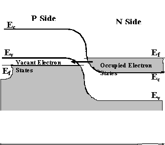
Figure 9: Energy band diagram for the tunnel diode showing the range of energies of electrons on the n side that can tunnel to the p side
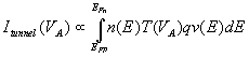
The tunneling current is determined by integrating the product of the electron density and the transmission coefficient over the aforementioned energy range so that:
 (25)
where:
n (E) = f(E) D(E) is the concentration of electrons on the n side in the energy range E and E + dE
(25)
where:
n (E) = f(E) D(E) is the concentration of electrons on the n side in the energy range E and E + dE
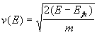 is the thermal velocity of the tunneling electrons of energy E, and
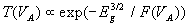 is the tunneling probability of the electron,
where
is the tunneling probability of the electron,
where 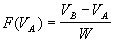 , where W is the width of the depletion region.
The I-V graph of the tunnel diode is determined by calculating the total current, which includes the tunneling current as determined in equation (25) as well as the standard forward biased diode current in equation (15) so that:
, where W is the width of the depletion region.
The I-V graph of the tunnel diode is determined by calculating the total current, which includes the tunneling current as determined in equation (25) as well as the standard forward biased diode current in equation (15) so that:
 (26)
The total current computed as per equation (24) is plotted in the I-V graph at the bottom right of the screen. The two cases where the tunnel diode is used in a "simple circuit" or a "circuit with resistance" result in different I-V graphs (See Figure 6a and 6b) for reasons discussed in the previous section.
The formalism presented above describes the equations that have been used to model the various p-n junction devices that have been simulated in this program. There are several simplifying assumptions made in these models, identical to the ones that are typically made in several standard texts in semiconductor or solid state physics.
IV. LIMITATIONS OF THE SIMULATION
While the Semiconductor Device Simulator is designed to enable the student to learn about energy bands in p-n junction devices and how these can be used to explain the electrical and spectral characteristics of these devices, the simulation is not accurate in certain situations.
The calculation of the electron and hole concentrations on either side of the p-n junction are not valid for a partially compensated semiconductor. It assumes that all the acceptors and donors are completely ionized. The simulation also assumes that the semiconductor has a direct band gap. Silicon for instance, which is the default semiconductor used in the simulation has an indirect band gap and hence is not suitable for making LEDs. While the program flashes the user a message indicating that silicon is not typically used to make LEDs, the user is not provided with any reasons as to why this is the case. The temperature dependence of the I-V characteristics are not completely accurate for all the semiconductor materials. The program does not take into account the temperature dependence of the energy gap. The temperature dependence for the electron and hole mobilities is assumed to follow the T-3/2 dependence, although this behavior is true only for silicon. For indirect semiconductors, the intensity of the light emitted by LEDs increases dramatically at lower temperatures. This is because in LEDs made out of indirect semiconductors, the phonon modes are frozen out at very low temperatures (i.e. no energy is lost to lattice vibrations), consequently the energy emitted when the electrons and holes recombine is all given out in the form of light, thereby increasing its intensity. In fact, a change in both the frequency as well as the intensity of light have been documented when a GaP (Gallium Phosphide) LED, doped with As (Arsenic) is immersed in liquid nitrogen9. The authors, however, caution that LEDs with multiple emission peaks arising from an introduction of impurities can exhibit more complex temperature effects. Another aspect of the simulation that could be potentially misleading is the intensity spectrum of the LEDs. The intensity spectrum is plotted on a logarithmic scale (although no such indication is provided to the user in the program). So colors that would not normally be visible to the naked eye, or even through a spectroscope are shown to be emitted in the intensity spectrum. For instance, an LED that is simulated using GaP as the semiconductor material, is shown to emit blue and ultraviolet light in its spectrum in addition to green light which has the greatest intensity. Since the intensity spectrum is on a logarithmic scale, the slightly lower intensity bar on the spectrum for blue compared to green represents an intensity value which is several orders of magnitude smaller, and hence would not be visible in a real experiment. Another feature of the intensity spectrum is that the lowest value of the energy (frequency) of emitted light corresponds to that of the energy gap. This is only valid under the idealized assumption that no donor or acceptor states exist within the band gap which participate in the transitions. This assumption is not true for actual LEDs. Indeed, semiconductor materials used to make LEDs are often doped with nitrogen, phosphorous, arsenic etc. to introduce these additional states, and alter their spectral characteristics. The resulting intensity spectrum of an actual LED, thus contains colors that have both energies, slightly higher and slightly lower than the band gap energy. The simulation does not show this feature. Also in the simulation, the color of light emitted by the LED in the diagram does not always commensurate with that on the spectrum. While the former is meant to be a visual indication that the LED emits light, the latter can be used for semi-quantitative analysis.
In spite of all the aforementioned anomalies and approximations in the models used, we believe that the Semiconductor Device Simulator can serve as a useful pedagogical tool. If the following section we present a brief tutorial on how the program could be used by students in the classroom.
V. A BRIEF TUTORIAL
The Semiconductor Device Simulator program was primarily designed to reach introductory students who do not have a strong background in higher level mathematics or physics. Consequently, all the mathematical computations are not visible to the user. The program, however, does provide powerful visual representations of how the energy band, I-V curves, and intensity spectra of p-n junction devices are interrelated and dependent upon other external factors that the user can vary. Hence, the program can be used by students over a range of academic levels. In the Solids and Light7 instructional unit, the program is used by introductory students who are led through a sequence of steps so that they can explain their experimental observations using the program. In this section, however, we outline some simple activities that would be suitable for students at a slightly higher level than the ones for whom the program was originally designed. We believe that many of the activities that are described below could also be adapted to students at introductory levels.
Step 1: Selecting the Semiconductor
The opening screen of the program is seen in Figure 1. Students begin by choosing the semiconductor from the Device menu in the top menu bar. Using this menu, students could also read off the various parameters associated with each of the semiconductors provided. This knowledge would enable students to choose a correct semiconductor that best matches the application desired. More advanced students could create their own hypothetical semiconductor. Students could be supplied with a set of performance requirements of the device and could be expected to work backwards to determine the semiconductor that would best meet these requirements. E.g. The semiconductor that would most likely be used to create:
(26)
The total current computed as per equation (24) is plotted in the I-V graph at the bottom right of the screen. The two cases where the tunnel diode is used in a "simple circuit" or a "circuit with resistance" result in different I-V graphs (See Figure 6a and 6b) for reasons discussed in the previous section.
The formalism presented above describes the equations that have been used to model the various p-n junction devices that have been simulated in this program. There are several simplifying assumptions made in these models, identical to the ones that are typically made in several standard texts in semiconductor or solid state physics.
IV. LIMITATIONS OF THE SIMULATION
While the Semiconductor Device Simulator is designed to enable the student to learn about energy bands in p-n junction devices and how these can be used to explain the electrical and spectral characteristics of these devices, the simulation is not accurate in certain situations.
The calculation of the electron and hole concentrations on either side of the p-n junction are not valid for a partially compensated semiconductor. It assumes that all the acceptors and donors are completely ionized. The simulation also assumes that the semiconductor has a direct band gap. Silicon for instance, which is the default semiconductor used in the simulation has an indirect band gap and hence is not suitable for making LEDs. While the program flashes the user a message indicating that silicon is not typically used to make LEDs, the user is not provided with any reasons as to why this is the case. The temperature dependence of the I-V characteristics are not completely accurate for all the semiconductor materials. The program does not take into account the temperature dependence of the energy gap. The temperature dependence for the electron and hole mobilities is assumed to follow the T-3/2 dependence, although this behavior is true only for silicon. For indirect semiconductors, the intensity of the light emitted by LEDs increases dramatically at lower temperatures. This is because in LEDs made out of indirect semiconductors, the phonon modes are frozen out at very low temperatures (i.e. no energy is lost to lattice vibrations), consequently the energy emitted when the electrons and holes recombine is all given out in the form of light, thereby increasing its intensity. In fact, a change in both the frequency as well as the intensity of light have been documented when a GaP (Gallium Phosphide) LED, doped with As (Arsenic) is immersed in liquid nitrogen9. The authors, however, caution that LEDs with multiple emission peaks arising from an introduction of impurities can exhibit more complex temperature effects. Another aspect of the simulation that could be potentially misleading is the intensity spectrum of the LEDs. The intensity spectrum is plotted on a logarithmic scale (although no such indication is provided to the user in the program). So colors that would not normally be visible to the naked eye, or even through a spectroscope are shown to be emitted in the intensity spectrum. For instance, an LED that is simulated using GaP as the semiconductor material, is shown to emit blue and ultraviolet light in its spectrum in addition to green light which has the greatest intensity. Since the intensity spectrum is on a logarithmic scale, the slightly lower intensity bar on the spectrum for blue compared to green represents an intensity value which is several orders of magnitude smaller, and hence would not be visible in a real experiment. Another feature of the intensity spectrum is that the lowest value of the energy (frequency) of emitted light corresponds to that of the energy gap. This is only valid under the idealized assumption that no donor or acceptor states exist within the band gap which participate in the transitions. This assumption is not true for actual LEDs. Indeed, semiconductor materials used to make LEDs are often doped with nitrogen, phosphorous, arsenic etc. to introduce these additional states, and alter their spectral characteristics. The resulting intensity spectrum of an actual LED, thus contains colors that have both energies, slightly higher and slightly lower than the band gap energy. The simulation does not show this feature. Also in the simulation, the color of light emitted by the LED in the diagram does not always commensurate with that on the spectrum. While the former is meant to be a visual indication that the LED emits light, the latter can be used for semi-quantitative analysis.
In spite of all the aforementioned anomalies and approximations in the models used, we believe that the Semiconductor Device Simulator can serve as a useful pedagogical tool. If the following section we present a brief tutorial on how the program could be used by students in the classroom.
V. A BRIEF TUTORIAL
The Semiconductor Device Simulator program was primarily designed to reach introductory students who do not have a strong background in higher level mathematics or physics. Consequently, all the mathematical computations are not visible to the user. The program, however, does provide powerful visual representations of how the energy band, I-V curves, and intensity spectra of p-n junction devices are interrelated and dependent upon other external factors that the user can vary. Hence, the program can be used by students over a range of academic levels. In the Solids and Light7 instructional unit, the program is used by introductory students who are led through a sequence of steps so that they can explain their experimental observations using the program. In this section, however, we outline some simple activities that would be suitable for students at a slightly higher level than the ones for whom the program was originally designed. We believe that many of the activities that are described below could also be adapted to students at introductory levels.
Step 1: Selecting the Semiconductor
The opening screen of the program is seen in Figure 1. Students begin by choosing the semiconductor from the Device menu in the top menu bar. Using this menu, students could also read off the various parameters associated with each of the semiconductors provided. This knowledge would enable students to choose a correct semiconductor that best matches the application desired. More advanced students could create their own hypothetical semiconductor. Students could be supplied with a set of performance requirements of the device and could be expected to work backwards to determine the semiconductor that would best meet these requirements. E.g. The semiconductor that would most likely be used to create:
- An LED with a peak wavelength of 645nm.
- A tunnel diode with a peak voltage of 0.4 V and valley voltage of 0.6V.
- A solar cell with an output voltage of 0.7V when irradiated with red light.
Step 2: Doping the Semiconductor
Next students have to dope the semiconductors with acceptors and donors (Figure 2). Each acceptor and donor "atom" that they implant, corresponds to an increment in the value of the acceptor and donor concentration. Students observe the change in the Fermi energy with the implantation of dopant atoms. Students could be asked to discuss the following:
- How does the Fermi energy change when we add donors? Acceptors?
- Does the Fermi energy increase/decrease linearly, exponentially, or logarithmically, with addition of donors/acceptors?
- What happens to the Fermi energy if we add both donors and acceptors to the same block? Why?
Step 3: Creating the P-N Junction
Having appropriately doped each semiconductor block, so that one of them is P type and the other N type, students bring the two semiconductor blocks together by clicking the "Connect" button, and then click the "Equilibrate" button (Figure 3) to make the Fermi levels on the two sides align. They also observe the built in voltage indicated in the energy band diagram, as well as the depletion layer width. At this point students could be asked:
- Why should the two Fermi levels align on the two sides
- How does the built in voltage change with the level of doping on each side
- How does the depletion layer width change with the doping on each side.
Step 4: Creating the Device
After creating the p-n junction, students can now create a device such as an LED, solar cell, or tunnel diode by clicking the "Choose Circuit" button, and choosing the menu options that follow. Each device can be used in two different modes. In case of the LED and tunnel diode, the "Simple Circuit" mode (Figure 4) allows the student to observe the behavior of the device when it is connected to an idealized variable voltage source, while in the "… with Resistance" mode (Figure 5), the device appears in a more realistic circuit where a potentiometer controls the flow of current through it.
In case of the LED, the student can change the voltage or resistance of the potentiometer and observe changes in the energy bands, I-V graph, and intensity spectrum. The students could be asked a variety of questions using LED simulations including :
- Why does the LED turn on only above a certain voltage?
- How are the intensity spectrum and turn on voltage of the LED related to the material used?
- What effect does the level of doping have on the turn-on voltage and intensity spectrum of an LED?
- How does the turn on voltage of the LED vary with temperature?
- What effect does increasing the junction area have on the I-V graph and intensity spectrum of the LED?
When the student attempts to create a tunnel diode, the program checks whether the Fermi energies on the n side and p side are above and below their respective conduction and valence band edges. If this condition is not satisfied, the program asks the user to increase the doping concentration. Unlike the LED, the I-V graphs of the tunnel diode are markedly different in the two modes (Figure 6 (a) and (b)). In the tunnel diode simulation, students could be asked to address the following questions:
- Why does the tunnel diode need a certain minimum level of doping concentration to operate.
- How do the peak and valley voltages change with the material of the tunnel diode?
- How do the peak and valley voltages change with the doping concentration of the tunnel diode?
- Why are the I-V graphs of the tunnel diode different in the two modes, while those of the LED are not?
If a solar cell is created, the student can either measure the output current and voltage of the device, or use it in a circuit to measure its I-V graph. In either case, the student can vary the intensity spectrum of the incident light, by clicking in the appropriate column in the intensity spectrum graph. A flash light of the appropriate color (which is the weighted average of the colors input in the intensity spectrum) appears indicating that the solar cell is irradiated. In the "Output Measurement" mode (Figure 7) the student can click on the terminals of the multimeter and make it toggle between an ammeter and voltmeter. The student can then measure the short circuit current and open circuit voltage of the solar cell, for different intensity spectra of the incident light. Pressing the "Keep" button below the intensity spectrum allows the student to preserve the output measurement settings for the solar cell for a given intensity spectrum, before examining the effects of a different intensity spectrum. Stored intensity spectra and the corresponding output measurements can be accessed using the "Data Sets" option in the pull down menu. The student could be asked to address the following questions:
- For a given solar cell, how does the open circuit voltage and short circuit current vary with the intensity spectrum?
- Is there a minimum energy of light that the solar cell must be irradiated with before it produces any current or voltage?
- How does this energy vary with the material of the solar cell?
- What influence does the doping concentration have on the performance of the solar cell?
When the student uses the "Solar Cell in Circuit" mode, she/he can observe how changes in both the intensity spectrum of the incident light, as well as the potentiometer resistance affect the I-V graph of the solar cell. Here, several I-V graphs can be generated for different intensity spectra. Students can address the following questions:
- How does the intensity spectrum affect the I-V graph of the solar cell circuit?
- How does the output power of the solar cell vary with the intensity spectrum?
- Which materials would be most suitable for creating solar cells which operate in sun light? in infrared light?
In this section we have presented a brief description of some of the activities that students could perform using the Semiconductor Device Simulator. The exercises outlined above could be used at the introductory level without the quantitative aspect of some of the questions. The program, has its limitations, and more advanced students would benefit to discuss the limitations of the models used to simulate these devices. In the following section we present some of the pedagogical applications of the program.
VI. PEDAGOGICAL APPLICATIONS
The Semiconductor Device Simulator program is useful pedagogically for several reasons. The computer program :
- Is completely interactive. Students must create their own semiconductor device by appropriately doping each piece of semiconductor, and choosing the circuit in which they wish to use the device. They must also change the input parameters -- the voltage applied and/or the spectrum of incident light.
- Can be integrated with hands-on experiments. The devices can be used in two types of simulated circuits. In one case the simulated circuit is simplified for pedagogical reasons. In the other case they can be used in a more complex but realistic circuit which is almost identical to one they may use in an experiment. We have used this program in a activity based environment where students build a real circuit using different electrical components on a breadboard. In this kind of a situation, students can use the program to explain their experimental results in terms of energy bands.
- Does not require any knowledge of higher level mathematics or physics. The program relies solely on visualization techniques to enable the student to learn the relationship between the energy bands of a semiconductor and the resulting electrical and spectral characteristics, with emphasis on qualitative reasoning and understanding. The student never sees the equations used in calculating the energy bands, intensity spectra, or currents, which were discussed in the previous section.
- Is versatile and can be used by students at virtually all levels from high school to advanced undergraduates in solid state physics or electrical engineering. High school and introductory college students can use the program to understand the electrical characteristics of some p-n junction devices and compare their results with experiments. More advanced students of solid state physics or electrical engineering can use the program to perform a ‘what if’ type of analysis by changing various parameters of these devices and observing the corresponding changes in band structure as well as the resulting changes in the electrical and spectral characteristics.
- Dynamically demonstrates the relationship between the energy bands in a p-n junction device and the resulting electrical and spectral characteristics. These characteristics can be observed on real devices in instructional laboratories. These relationships have so far only been shown in still pictures in text books.
- Allows the user to simulate changes in the semiconductor device including changes in dopant density, temperature, and junction area and observe the resulting changes in the electrical characteristics. Hence, the program fills a void for those students who were not able to study the behavior of individual devices without using more advanced circuit simulators.
VII. FEEDBACK FROM USERS
The program has been tested in various environments. We used the program in an introductory modern physics course taken primarily by secondary education majors at Kansas State University. The program was used by students in conjunction with hands-on activities in the class room with LEDs and solar cells and also in the laboratory with bipolar junction transistors and tunnel diodes.
We are currently field-testing the program in high schools and universities across the nation as a part of the "Solids and Light" instructional unit. The students use the program with accompanying hands-on activities, other programs, and written materials in the two-week instructional unit which uses LEDs as the pedagogical vehicle to convey concepts of energy bands in a solid and the emission of light due to electronic transitions. Students begin with the measurement the I-V graph of the LED and realize that it cannot be explained by Ohm’s law. This observation motivates the students to look at the LED more closely. Through a investigations of the LED, students learn that, unlike most other light sources that they may have encountered, the LED is a solid state device. Since solids are more complex than gases, because of closely packed atoms, the students attempt to begin by studying a gaseous light source. By observing gas lamps whose spectra are discrete lines, and using a computer program8, students empirically understand that electrons in gases can have only certain allowed energies. This idea is most conveniently represented by modeling an isolated gas atom by a square potential energy well. Since solids contain several atoms that are closely spaced, in this representation, a solid is an array of closely spaced potential energy wells. Another computer program10 enables students to observe the formation of energy bands in a solid. Having developed the idea of energy bands in a solid the students reinforce this concept through the observation of the continuous emission spectra of an LED. Finally students use the Semiconductor Device Simulator program to apply the energy band concept to explain both the electrical and spectral characteristics of the LED.
The program was also critiqued by the Visual Quantum Mechanics project’s national advisory board, consisting of high school and university faculty, and by other researchers in the field of physics education based in U.S, Europe and the Middle East.
VIII. SUMMARY
The Semiconductor Device Simulator program allows a user to observe the changes in the energy bands for a p-n junction device. The user begins by choosing semiconductor and doping it with the desired type of dopant. Two differently doped pieces of semiconductor are then brought together to create a p-n junction device - an LED, solar cell or a tunnel diode. The device can be used in a simulated simple circuit with a variable power supply or in a more realistic circuit with a battery, a resistance and a potentiometer. The user can change the voltage applied across the device and observe the resulting changes in band structure and the current as shown on an I-V graph. In case of the LED the user can also observe the spectrum of the emitted light. The user can change several parameters including the dopant density, the junction area, the temperature, and in case of the solar cell the intensity spectrum of the incident light. More advanced users can also create their own semiconductor with any desired energy band gap, carrier mobility and effective masses.
We believe that the program has several pedagogical applications at various levels due to its versatility and user friendliness. We have field tested the program in high school and university environments and the results have been very positive. We have incorporated some of the feedback that we received in the current version of the program. The program was awarded an honorable mention in the Computers in Physics journal’s Seventh Annual Education Software contest11 conducted by the AIP. The current version of the program for both the Windows and Macintosh platforms can be downloaded from our World Wide Web site http://www.phys.ksu.edu/perg/vqm.
FOOTNOTES
1 Supported by the National Science Foundation, under grant ESI 9452782.
2 More information about Visual Quantum Mechanics may be obtained at our World Wide Web site http://bluegiant.phys.ksu.edu.
3 Charles Kittel, Introduction to Solid State Physics, Sixth Edition, Wiley, New York, 1986.
4 Ben G. Streetman, Solid State Electronic Devices, Prentice Hall, Englewood Cliffs, 1972.
5 Mike. J. Cooke, Semiconductor Devices, Prentice Hall International, UK, 1990.
6 Sheng S. Li, Semiconductor Physical Electronics, Plenum Press, New York, 1993.
7 Lawrence T. Escalada, N. Sanjay Rebello, Dean A. Zollman, Solids & Light – An instructional Unit on Quantum Effects in LEDs, Physics Education Research Group, Kansas State University, 1996.
8 Atomic Spectroscopy computer program, Physics Education Research Group, Kansas State University, 1996.
9 A.B. Ellis, M.J. Geselbracht, B.J. Johnson, G.C. Lisensky, and W.R. Robinson, Teaching General Chemistry: A Materials Science Companion, Am. Chem. Soc., (1993) pp. 218-226.
10 Energy Band Creator computer program, Physics Education Research Group, Kansas State University, 1996.
11 Donnelly, D, CIP’s Seventh Annual Educational Software Contest: The Winners, Computers in Physics, Vol. 10, No. 6, Nov/Dec 1996, pp.532-541.